Monday, 28 April 2014

WEEK 7

Date: 17/3/14

Introduction

Hardware development is a parts of where all the components that has been tested will be installed according to the wiring diagram that designed in the previous week. This week, all works that relate with this matter will be discussed and shown clearly.

Objective
  • To install all the components related with the project.
  • To wire the components according to the wiring diagram that designed.
Problem Encountered

All works that made is based on the project design and wiring diagram that has been implemented before. Thus, it does not give any problem either before, during or after do this activities. However, all the wire connection and components is ensured installed on the right connection and arranged properly.

Project Description

The installation and wiring for this project is made separately. The following is the procedures to install and wire all the components that used in this project.

Step 1
  
Each part of component is installed one by one and arranged properly according to the project design but before that a surface of plywood need to painted to look nice and tidy. In this project, the plywood is used as base where all the components will be mounted on this plywood. The Figure 1 below shows the plywood that have been painted with black colour.

Figure 1: A surface of plywood that have been painted.

Step 2

When the paint is completely dry, all the components will mounted on the painted plywood and arranged according to the project design. Below is the figure that shows the components that have been arranged and mounted on the plywood.

Figure 2: A few components that have been completed mounted
on the painted plywood.
 
Step 3

After all the components completed mounted on the plywood, each part of component will be wired according to the wiring diagram and the result is such as Figure 3 below.

Figure 3: Each part of electrical and electronic is wired separately.

Step 4

Once all parts of electrical appliances is wired completely, a wiring job for the electronic part will be made. This part is made side by side to avoid any mistake in the wiring. Below is the figure that shows both parts of project that have been wired completely.
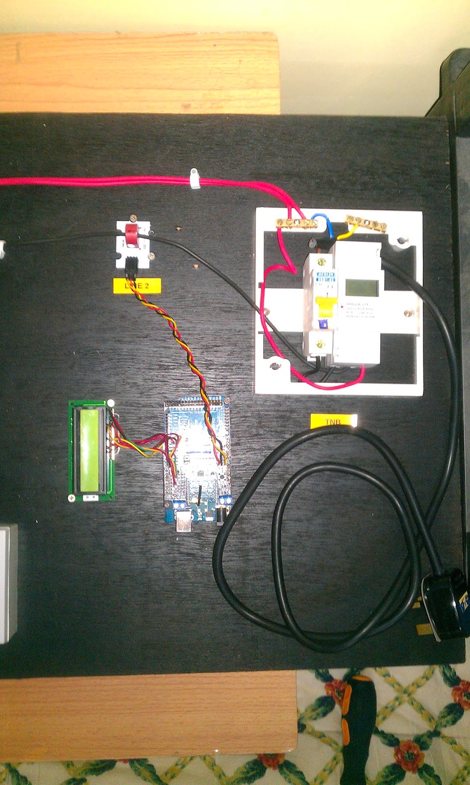
Figure 4: This parts are referred as pole based systems
and have been wired completely.
  
Figure 5: This parts are referred as consumer based systems
and have been wired completely.

All parts of the hardware have been installed and wired based on the project design and wiring diagram that have been designed before. Thus, the results that obtained from this activities is such as the figure that shown in the Project Outcome below.

Project Outcome

Figure 6: The end result for the hardware development part.
  
As a conclusion, all works done smoothly. Thus, for the other work that relate with the software development will be made in the next progress report.

Tuesday, 15 April 2014

WEEK 6

Date: 10/3/14

Introduction

Functional testing is a hardware testing process used within hardware development in which hardware is tested to ensure that it conforms with all requirements. Functional testing is a way of checking hardware to ensure that it has all the required functionality that's specified within its functional requirements. In this project (ETDMS), this process will be made on two main parts i.e. (1) hardware part and (2) software part. However, this process will be made in separately starting from the functional test for the hardware part and ended with the functional test for the software part. This week, the functional test for the hardware part will be made and discussed in details.

Objective
  • To makes a functional test on each part of hardware.
  • To shows all the results that obtained from the testing that has been made.
Problem Encountered

In this activity, it does not give any problem because all the information for each hardware parts has been identified in the previous week. Thus, the functional test can be made according to the information that has been obtained.

Project Description

Each part of the hardware is tested according to the list of the testing and inspection that mentioned below:-
  1. Visual inspection on each part of hardware.
  2. Continuity test.
  3. Polarity.
  4. Functional switching and Isolation.
This testing is made in two different situation i.e. (1) before connection of the supply and (2) with the supply connected. All the result that obtained from this test procedures is shown in the Project Outcome below.

Project Outcome

Table 1: Test Results - Hardware Parts

Based on the Table 1 above, it shows that all the components is functional correctly. Thus, the installation of hardware and wiring will be made and shown on the next progress report.  

Sunday, 13 April 2014

WEEK 5

Date: 3/3/14

Introduction

In develops a project, aside from design a gantt chart, block diagram and flow chart, the other thing that need to made is design a circuit diagram. The circuit diagram will become as a reference to wire the overall project according to the project that needed. Thus, to design the circuit diagram, a suitable software need to used to makes the circuit diagram that designed clear, standard and able to understood by others. Generally, in the real applications, the circuit drawing or technical drawing is designed by using AutoCAD software, but since a skill to use that software are quite weak, one of the initiative/solution for that problem is by using a Microsoft Office Visio. From this solution, the circuit diagram that designed will look clear and easy for anyone to understand the drawing.

Objective 
  • To design the circuit diagram based on the actual project applications.
  • To shows the circuit diagram for each part of hardware and for the overall part of hardware (complete circuit).
Problem Encountered

From this activity, the problem that encountered is in terms of to read and understand each datasheet. It is because all the information that given in the datasheet need to understood which is for the purposes (1) to avoid from any damage on the component, (2) to connect/wire exactly on each terminal board/port that should be connected only. On the other hand, the methods about how to use the Microsoft Office Visio software does not become a problem because this software is always used in designing the block diagram, flow chart and etc.

Project Description

First of all, once all the data about each part of hardware that need to known is identified correctly, part by part of the hardware will be wired separately. Below is the methods to wire each part of the component used in the Electricity Theft Detection Metering System:-

A) LINE 1
  
1. Plug Top 13A wiring details

Figure 1: Method to wire Plug Top 13A

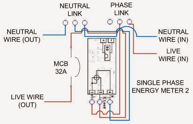
2. Wiring diagram for Single Phase Energy Meter and MCB 32A

Figure 2: Method to wire Single Phase Energy Meter and MCB 32A (mounted in Distribution Box 1)

3. Wiring diagram for Controller Board 1

Figure 3: Method to wire Current Sensor and LCD module on the IO Expansion Shield

Note:-
The IO Expansion Shield and RF Module (transmitter) no need to wired because both of this components is only need to placed/mounted on the socket that has been provided.

B) BETWEEN LINE 1 & LINE 2

1. Load 1 wiring details

Figure 4: One switch control one light (Load 1)
 
C) LINE 2

1. Wiring diagram for Single Phase Energy Meter and MCB 32A

Figure 5: Method to wire Single Phase Energy Meter and MCB 32A (mounted in Distribution Box 2)

2. Load 2 wiring details

Figure 6: One switch control two lights (Load 2)

3. Wiring diagram for Controller Board 2

Figure 7: Method to wire Current Sensor, LCD module and Bluetooth module on the IO Expansion shield

Note:-
The IO Expansion Shield, RF Module (receiver) and BTBee Explorer Regulated no need to wired because this components is only need to placed/mounted on the socket/shield that has been provided.
 
Project Outcome

The circuits that designed for each part of component will be combined according to the project requirements. Below is the complete circuit for Electricity Theft Detection Metering System that obtained from this activity:-

Figure 8: A circuit diagram for Electricity Theft Detection Metering System (complete circuit)

From the circuit diagram that has been designed above, it will be used as a reference for the hardware development work. Before that, each part of the circuit will be tested to ensure it works well. This tasks will be discussed on the next progress report from broad to narrow.

Tuesday, 8 April 2014

WEEK 4

Date: 26/2/14

Introduction

As mentioned in the previous week, this week a existing flow chart will be redesigned exactly based on the project that are being made. The flow chart need to redesigned because the flow chart that made in the previous FYP session (FYP 1) is only a draft and not the exact flow chart that used in the project. However, the changes that made is not totally different with the existing flow chart. The function/flow of project is still similar as proposed in the FYP 1.

Objective 
  • To redesign flow chart exactly with the project that developed.
Problem Encountered

To create the flow chart, several factors need to be considered such as in term of their symbol. The symbols of flow chart is very important to make a readers understand the flow of project that made. Thus, the selection of flow chart symbol should be correct according to the function/flow of project that made. However, all this problem has been solved in the previous FYP session (FYP 1) by makes some research in website and other sources.

Project Description 

The flow chart that made is based on the existing flow chart in the previous post for FYP 1 on WEEK 5 and for the other thing is according to the project that are being implemented. The result that obtained is such the project outcome below.

Project Outcome

Below is the result that obtained from this activity:-

Figure 1: Actual Process Flow Chart (redesigned)
          
The Figure 1 above is the actual flow chart that has been redesigned according to the function/flow of project that made. Others information in term of their circuit diagram either for each part of hardware or combination for all parts of hardware (complete circuit) will be discussed in details on next progress report.   

Wednesday, 2 April 2014

WEEK 3

Date: 17/2/14

Introduction

A block diagram become one of the important part in develop a project. This week the existing block diagram will be re-designed according exactly with the project that developed. The block diagram need to re-designed because some of the component that listed in FYP 1 was changed with the other component. The changes that made is for the purposes to reduce project costing and also to make the project become more efficient and easy to used.

Objective 
  • To re-design block diagram exactly with the project that developed.
Problem Encountered

From this activity, it does not give much problem because the block diagram that re-designed is still based on the previous block diagrams and only at the certain part/block is changed i.e. according to the two main criteria which are (1) the components that replaced and (2) based on the actual project.

Project Description 

The block diagram is re-designed by using a Microsoft Visio software. Each part of block diagrams is labelled and connected according to the project flow from the beginning until to the end of the project flow. The block diagrams that has been re-designed will be shown in the project outcome below.

Project Outcome

Figure 1: Block Diagram (re-designed)

The Figure 1 above is the block diagram that has been re-designed according to the exact project flow that developed in FYP 2. The function/flow of Electricity Theft Detection Metering System is based on this block diagram. Others progress will be continued on next week.